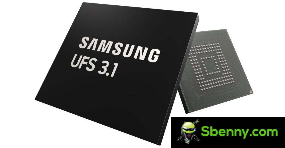
Samsung has announced that it has started mass production of its Automotive UFS 3.1, which will be available to global automakers and component manufacturers later this year. This storage space will have capacities of 128, 256 and 512 GB. The 256GB model, for example, will offer sequential read speeds of up to 2,000MB/s and sequential write speeds of up to 700MB/s.
Samsung claims that this UFS 3.1 has the lowest power consumption in the industry, consuming 33% less energy than the previous generation product.
In case you’re wondering what the difference is between UFS that goes in phones and one that goes in cars, it’s the endurance of the thing. Automotive UFS 3.1 has been AEC-Q100 Grade2 certified, which ensures stable performance over a wide temperature range of -40°C to 105°C (-40°F to 221°F). This will be well outside the range in which smartphone chips should work.
This storage is optimized for In-Vehicle Infotainment (IVI) and will pair with other Samsung parts such as Auto LPDDR5X, Auto GDDR6 and Exynos Auto V920. This chipset has been selected as the IVI brains for the new generation cars of the Hyundai Group. Samsung is already supplying some chips to Tesla (14nm from its Texas foundry), but the two companies are also negotiating a supply of 5nm chips for Full Self Driving. You can follow more automotive news on our sister site ArenaEV.
However, Samsung will also supply its automotive UFS 3.1 for use in ADAS – Advanced Driver Assistance Systems – and has already received ASPICE Level 2 certification from customers and C&BIS.
“Samsung’s new UFS 3.1 solution addresses a broad range of customer needs for optimized IVI systems, driving forward next-generation memory trends that demand higher ESG standards. We aim to expand our presence in the automotive semiconductor market, following the introduction of our UFS 3.1 solution for Advanced Driver Assistance Systems (ADAS),” said Hyunduk Cho, vice president of the memory product planning team at Samsung Electronics.
Start a new Thread